Approaches to Nano Tech


Gist


Top-Down Approach

Starts with larger structures and breaks them down to the nanoscale.

Techniques

• Lithography: Uses light or electron beams to create tiny patterns on a surface.

• Chemical etching: Uses chemicals to remove unwanted material, leaving behind nanostructures.

• Mechanical machining: Uses very small tools to create precise shapes at the nanoscale.

Bottom-Up Approach:
Builds structures from the bottom up, atom by atom or molecule by molecule.
Techniques:

• Chemical self-assembly: Molecules are designed to self-assemble into desired structures.

• Biomimetics: Mimicking nature's processes to create nanostructures. For instance, studying how viruses assemble themselves.

• Supramolecular assembly: Designing molecules that can link together to form larger structures.

Choosing the Approach
• The choice between these approaches depends on the desired nanostructure and its intended application.

• Top-down methods offer greater control over precise shapes and patterns but can be complex and expensive.

• Bottom-up methods can be more scalable and potentially lead to self-repairing structures, but achieving precise control can be challenging.

The Future of Nanotech
• Combining these approaches with advancements in areas like AI and computational modeling is leading to significant progress in nanotechnology.

• Potential applications span various fields like medicine, electronics, energy, materials science, and environmental remediation.

• Challenges and Considerations:
• Ethical considerations regarding potential environmental and health risks of nanomaterials need careful evaluation.

• Safe and responsible development of nanotechnologies is crucial for maximizing their benefits.

• Overall, understanding these approaches provides a glimpse into the exciting world of nanotechnology and its potential to revolutionize various fields.


Summary


• Bottom-Up Approaches: Involve building nanostructures from atomic or molecular constituents, offering precise control but requiring careful design. Techniques include molecular self-assembly, chemical vapor deposition (CVD), and molecular beam epitaxy (MBE).

• Top-Down Approaches: Carve nanostructures out of bulk materials, offering scalability but with less precision. Techniques include lithography and etching, crucial for semiconductor manufacturing and creating nanostructured surfaces.

• Hybrid Approaches: Combine elements of bottom-up and top-down techniques to achieve complex nanostructures with enhanced functionality. Examples include template-assisted synthesis and directed self-assembly (DSA), offering precise patterning and large-scale fabrication capabilities.

• Applications: Nanotechnology finds applications across sectors such as electronics, medicine, energy, and the environment. Examples include faster and more efficient electronic devices, targeted drug delivery in healthcare, and improved renewable energy technologies.


Detailed content


Introduction

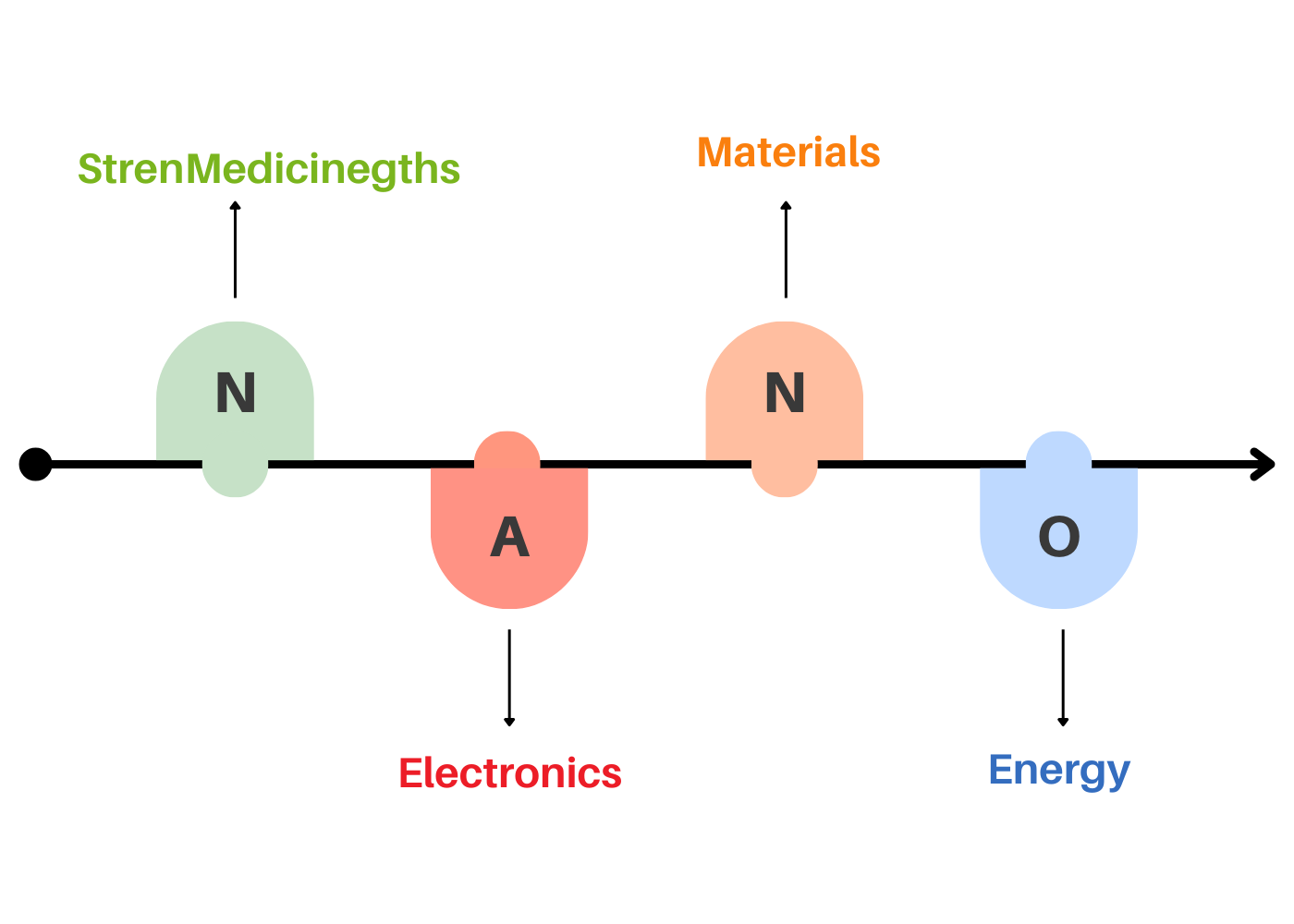
Nanotechnology, the manipulation of matter at the nanoscale, holds immense promise for revolutionizing various fields, from medicine and electronics to materials science and energy. At the heart of nanotechnology lie diverse approaches aimed at fabricating, characterizing, and utilizing materials and devices at the nanoscale. In this comprehensive exploration, we delve into the various approaches to nanotechnology, encompassing bottom-up and top-down methods, self-assembly techniques, and hybrid approaches. Each approach brings unique advantages and challenges, shaping the landscape of nanotechnology research and applications.

1.Bottom-Up Approaches

Bottom-up approaches involve building nanostructures from atomic or molecular constituents, enabling precise control over structure and properties. Key techniques include molecular self-assembly, chemical vapor deposition (CVD), and molecular beam epitaxy (MBE).

1.1 Molecular Self-Assembly

Molecular self-assembly harnesses the inherent properties of molecules to spontaneously organize into ordered structures. Examples include DNA nanotechnology, where DNA molecules serve as programmable building blocks, and peptide self-assembly, exploiting the folding properties of peptides to create nanostructures. Self-assembly offers high precision and scalability but requires careful design and control of molecular interactions.

1.2 Chemical Vapor Deposition (CVD)

CVD involves depositing thin films of materials onto substrates by exposing precursor gases to a heated substrate surface, where chemical reactions occur to form the desired material. CVD enables precise control over film thickness and composition and is widely used in semiconductor manufacturing and thin-film coatings. However, achieving uniformity and purity at the nanoscale poses challenges.

1.3 Molecular Beam Epitaxy (MBE)

MBE relies on the precise deposition of atoms or molecules onto a substrate under ultra-high vacuum conditions. By controlling the flux of incoming species, MBE allows for the growth of atomically thin layers with exceptional control over crystal structure and composition. MBE is crucial for fabricating semiconductor heterostructures and quantum dots but requires sophisticated equipment and expertise.

2.Top-Down Approaches

Top-down approaches involve carving nanostructures out of bulk materials, often using lithography or etching techniques. While less precise than bottom-up methods, top-down approaches offer scalability and compatibility with existing manufacturing processes.

2.1 Lithography

Lithography is a cornerstone technique in nanofabrication, capable of defining nanoscale patterns on surfaces with high precision. Techniques such as photolithography, electron beam lithography (EBL), and nanoimprint lithography (NIL) enable the creation of features down to a few nanometers. Lithography underpins the semiconductor industry, enabling the production of integrated circuits and microelectromechanical systems (MEMS).

2.2 Etching

Etching techniques selectively remove material from a substrate to sculpt nanostructures. Wet etching uses liquid chemical solutions to dissolve unwanted material, while dry etching methods such as reactive ion etching (RIE) and plasma etching rely on reactive gases to achieve high selectivity and anisotropy. Etching is crucial for defining device geometries in semiconductor fabrication and creating nanostructured surfaces for applications in optics and catalysis.

3.Hybrid Approaches

Hybrid approaches combine elements of bottom-up and top-down techniques to achieve complex nanostructures with enhanced functionality.

3.1 Template-Assisted Synthesis

Template-assisted synthesis combines the precision of bottom-up assembly with the scalability of top-down processing. Templates such as nanoporous membranes or lithographically patterned substrates guide the growth of nanostructures, enabling precise control over size, shape, and orientation. Template-assisted synthesis is used in the fabrication of nanowires, nanotubes, and nanoparticle arrays for applications in electronics, sensing, and energy conversion.

3.2 Directed Self-Assembly (DSA)

DSA combines self-assembly principles with top-down patterning to achieve large-scale patterning of nanoscale features. Block copolymers, consisting of two or more chemically distinct polymer blocks, spontaneously organize into periodic nanostructures when deposited onto patterned substrates. DSA enables the creation of dense, regular patterns with feature sizes below the resolution limit of conventional lithography, offering potential benefits for semiconductor device fabrication and data storage technologies.

4.Applications and Future Directions

The diverse approaches to nanotechnology pave the way for numerous applications across sectors.

4.1 Electronics and Photonics

Nanotechnology enables the miniaturization of electronic and photonic devices, leading to faster, more efficient technologies. Quantum dots, nanowires, and 2D materials hold promise for next-generation transistors, sensors, and displays.

4.2 Medicine and Healthcare

Nanomedicine offers targeted drug delivery, imaging, and diagnostics at the molecular level, revolutionizing healthcare. Nanoparticles, liposomes, and nanotubes enable precise control over drug release kinetics and tissue targeting, enhancing therapeutic efficacy and reducing side effects.

4.3 Energy and Environment

Nanotechnology plays a crucial role in renewable energy generation, storage, and efficiency improvement. Nanostructured materials enhance the performance of solar cells, batteries, and catalysts, while nanomembranes enable efficient water purification and desalination.

Conclusion

Approaches to nanotechnology encompass a diverse array of techniques, each with unique advantages and challenges. Bottom-up methods offer precise control over nanostructures but require careful design and synthesis, while top-down approaches enable scalability and compatibility with existing manufacturing processes. Hybrid approaches combine the strengths of both paradigms, unlocking new opportunities for complex nanostructure fabrication. As nanotechnology continues to advance, interdisciplinary collaboration and innovation will drive the development of transformative technologies with profound societal impact.


தமிழில் விரிவான உள்ளடக்கம்


அறிமுகம்

நானோ தொழில்நுட்பம், நானோ அளவிலான பொருளின் கையாளுதல், மருத்துவம் மற்றும் மின்னணுவியல் முதல் பொருள் அறிவியல் மற்றும் ஆற்றல் வரை பல்வேறு துறைகளில் புரட்சியை ஏற்படுத்துவதற்கான மகத்தான வாக்குறுதியைக் கொண்டுள்ளது. நானோ தொழில்நுட்பத்தின் மையத்தில் நானோ அளவிலான பொருட்கள் மற்றும் சாதனங்களை உருவாக்குதல், வகைப்படுத்துதல் மற்றும் பயன்படுத்துதல் ஆகியவற்றை நோக்கமாகக் கொண்ட பல்வேறு அணுகுமுறைகள் உள்ளன. இந்த விரிவான ஆய்வில், நானோ தொழில்நுட்பத்திற்கான பல்வேறு அணுகுமுறைகளை நாங்கள் ஆராய்வோம், கீழே இருந்து மேல் மற்றும் மேல்-கீழ் முறைகள், சுய-அசெம்பிளி நுட்பங்கள் மற்றும் கலப்பின அணுகுமுறைகளை உள்ளடக்கியது. ஒவ்வொரு அணுகுமுறையும் தனித்துவமான நன்மைகள் மற்றும் சவால்களைக் கொண்டுவருகிறது, நானோ தொழில்நுட்ப ஆராய்ச்சி மற்றும் பயன்பாடுகளின் நிலப்பரப்பை வடிவமைக்கிறது.

1.கீழ்-மேல் அணுகுமுறைகள்

பாட்டம்-அப் அணுகுமுறைகள் அணு அல்லது மூலக்கூறு கூறுகளிலிருந்து நானோ கட்டமைப்புகளை உருவாக்குவதை உள்ளடக்கியது, கட்டமைப்பு மற்றும் பண்புகளின் மீது துல்லியமான கட்டுப்பாட்டை செயல்படுத்துகிறது. முக்கிய நுட்பங்களில் மூலக்கூறு சுய-அசெம்பிளி, இரசாயன நீராவி படிவு (CVD) மற்றும் மூலக்கூறு கற்றை எபிடாக்ஸி (MBE) ஆகியவை அடங்கும்.

1.1 மூலக்கூறு சுய-அசெம்பிளி

மூலக்கூறுகளின் உள்ளார்ந்த பண்புகளை தன்னிச்சையாக ஒழுங்குபடுத்தப்பட்ட கட்டமைப்புகளாக ஒழுங்கமைக்க மூலக்கூறு சுய-அசெம்பிளி பயன்படுத்துகிறது. எடுத்துக்காட்டுகளில் டிஎன்ஏ நானோ தொழில்நுட்பம் அடங்கும், அங்கு டிஎன்ஏ மூலக்கூறுகள் நிரல்படுத்தக்கூடிய கட்டுமானத் தொகுதிகளாக செயல்படுகின்றன, மற்றும் பெப்டைட் சுய-அசெம்பிளி, பெப்டைட்களின் மடிப்பு பண்புகளை நானோ கட்டமைப்புகளை உருவாக்குகின்றன. சுய-அசெம்பிளி அதிக துல்லியம் மற்றும் அளவிடுதல் ஆகியவற்றை வழங்குகிறது ஆனால் மூலக்கூறு தொடர்புகளின் கவனமாக வடிவமைப்பு மற்றும் கட்டுப்பாடு தேவைப்படுகிறது.

1.2 இரசாயன நீராவி படிவு (CVD)

CVD என்பது ஒரு சூடான அடி மூலக்கூறு மேற்பரப்பில் முன்னோடி வாயுக்களை வெளிப்படுத்துவதன் மூலம் அடி மூலக்கூறுகளில் மெல்லிய படலங்களை வைப்பதை உள்ளடக்குகிறது, அங்கு வேதியியல் எதிர்வினைகள் விரும்பிய பொருளை உருவாக்குகின்றன. சிவிடி பட தடிமன் மற்றும் கலவை மீது துல்லியமான கட்டுப்பாட்டை செயல்படுத்துகிறது மற்றும் குறைக்கடத்தி உற்பத்தி மற்றும் மெல்லிய-பட பூச்சுகளில் பரவலாகப் பயன்படுத்தப்படுகிறது. இருப்பினும், நானோ அளவிலான சீரான தன்மை மற்றும் தூய்மையை அடைவது சவால்களை ஏற்படுத்துகிறது.

1.3 மாலிகுலர் பீம் எபிடாக்ஸி (MBE)

MBE ஆனது அதி-உயர் வெற்றிட நிலைமைகளின் கீழ் ஒரு அடி மூலக்கூறு மீது அணுக்கள் அல்லது மூலக்கூறுகளின் துல்லியமான படிவுகளை நம்பியுள்ளது. உள்வரும் உயிரினங்களின் ஓட்டத்தைக் கட்டுப்படுத்துவதன் மூலம், படிக அமைப்பு மற்றும் கலவையின் மீது விதிவிலக்கான கட்டுப்பாட்டுடன் அணு மெல்லிய அடுக்குகளின் வளர்ச்சியை MBE அனுமதிக்கிறது. குறைக்கடத்தி ஹீட்டோரோஸ்ட்ரக்சர்கள் மற்றும் குவாண்டம் புள்ளிகளை உருவாக்குவதற்கு MBE முக்கியமானது, ஆனால் அதிநவீன உபகரணங்கள் மற்றும் நிபுணத்துவம் தேவைப்படுகிறது.

2. மேல்-கீழ் அணுகுமுறைகள்

மேல்-கீழ் அணுகுமுறைகள் மொத்தப் பொருட்களிலிருந்து நானோ கட்டமைப்புகளை செதுக்குவதை உள்ளடக்கியது, பெரும்பாலும் லித்தோகிராபி அல்லது செதுக்கும் நுட்பங்களைப் பயன்படுத்துகிறது. கீழ்நிலை முறைகளைக் காட்டிலும் குறைவான துல்லியமானதாக இருந்தாலும், மேல்-கீழ் அணுகுமுறைகள், தற்போதுள்ள உற்பத்தி செயல்முறைகளுடன் அளவிடுதல் மற்றும் இணக்கத்தன்மையை வழங்குகின்றன.

2.1 லித்தோகிராபி

லித்தோகிராஃபி என்பது நானோ ஃபேப்ரிகேஷனில் ஒரு மூலக்கல்லாகும், இது அதிக துல்லியத்துடன் மேற்பரப்புகளில் நானோ அளவிலான வடிவங்களை வரையறுக்கும் திறன் கொண்டது. ஃபோட்டோலித்தோகிராபி, எலக்ட்ரான் பீம் லித்தோகிராபி (ஈபிஎல்) மற்றும் நானோஇம்ப்ரிண்ட் லித்தோகிராபி (என்ஐஎல்) போன்ற நுட்பங்கள் சில நானோமீட்டர்கள் வரை அம்சங்களை உருவாக்க உதவுகின்றன. லித்தோகிராபி குறைக்கடத்தி தொழிற்துறையை ஆதரிக்கிறது, ஒருங்கிணைந்த சுற்றுகள் மற்றும் மைக்ரோ எலக்ட்ரோ மெக்கானிக்கல் அமைப்புகளின் (MEMS) உற்பத்தியை செயல்படுத்துகிறது.

2.2 பொறித்தல்

பொறித்தல் நுட்பங்கள் நானோ கட்டமைப்புகளை செதுக்க ஒரு அடி மூலக்கூறிலிருந்து பொருளைத் தேர்ந்தெடுத்து அகற்றுகின்றன. ஈரமான பொறித்தல் தேவையற்ற பொருட்களைக் கரைக்க திரவ இரசாயன தீர்வுகளைப் பயன்படுத்துகிறது, அதே சமயம் ரியாக்டிவ் அயன் எச்சிங் (RIE) மற்றும் பிளாஸ்மா பொறித்தல் போன்ற உலர் பொறித்தல் முறைகள் உயர் தேர்வு மற்றும் அனிசோட்ரோபியை அடைய எதிர்வினை வாயுக்களை நம்பியுள்ளன. செமிகண்டக்டர் ஃபேப்ரிகேஷனில் சாதன வடிவவியலை வரையறுப்பதற்கும் ஒளியியல் மற்றும் வினையூக்கத்தில் பயன்பாடுகளுக்கு நானோ கட்டமைக்கப்பட்ட மேற்பரப்புகளை உருவாக்குவதற்கும் பொறித்தல் முக்கியமானது.

3.ஹைப்ரிட் அணுகுமுறைகள்

கலப்பின அணுகுமுறைகள் மேம்பட்ட செயல்பாட்டுடன் சிக்கலான நானோ கட்டமைப்புகளை அடைய கீழ்-மேல் மற்றும் மேல்-கீழ் நுட்பங்களின் கூறுகளை இணைக்கின்றன.

3.1 டெம்ப்ளேட்-உதவி தொகுப்பு

டெம்ப்ளேட்-உதவி தொகுப்பு, மேல்-கீழ் செயலாக்கத்தின் அளவிடுதலுடன் கீழ்-மேல் சட்டசபையின் துல்லியத்தை ஒருங்கிணைக்கிறது. நானோபோரஸ் சவ்வுகள் அல்லது லித்தோகிராஃபிக் வடிவிலான அடி மூலக்கூறுகள் போன்ற வார்ப்புருக்கள் நானோ கட்டமைப்புகளின் வளர்ச்சிக்கு வழிகாட்டி, அளவு, வடிவம் மற்றும் நோக்குநிலை ஆகியவற்றின் மீது துல்லியமான கட்டுப்பாட்டை செயல்படுத்துகிறது. மின்னணுவியல், உணர்திறன் மற்றும் ஆற்றல் மாற்றத்திற்கான பயன்பாடுகளுக்கான நானோவாய்கள், நானோகுழாய்கள் மற்றும் நானோ துகள்களின் வரிசைகளை உருவாக்குவதற்கு டெம்ப்ளேட்-உதவி தொகுப்பு பயன்படுத்தப்படுகிறது.

3.2 Directed Self-Assembly (DSA)

நானோ அளவிலான அம்சங்களின் பெரிய அளவிலான வடிவமைப்பை அடைய டிஎஸ்ஏ சுய-அசெம்பிளி கொள்கைகளை டாப்-டவுன் பேட்டர்னிங்குடன் ஒருங்கிணைக்கிறது. இரண்டு அல்லது அதற்கு மேற்பட்ட வேதியியல் ரீதியாக வேறுபட்ட பாலிமர் தொகுதிகளைக் கொண்ட பிளாக் கோபாலிமர்கள், வடிவமைக்கப்பட்ட அடி மூலக்கூறுகளில் டெபாசிட் செய்யும் போது தன்னிச்சையாக அவ்வப்போது நானோ கட்டமைப்புகளாக ஒழுங்கமைக்கப்படுகின்றன. DSA ஆனது, வழக்கமான லித்தோகிராஃபியின் தெளிவுத்திறன் வரம்பிற்குக் கீழே அம்ச அளவுகளுடன் அடர்த்தியான, வழக்கமான வடிவங்களை உருவாக்க உதவுகிறது, குறைக்கடத்தி சாதனம் புனையமைப்பு மற்றும் தரவு சேமிப்பக தொழில்நுட்பங்களுக்கான சாத்தியமான நன்மைகளை வழங்குகிறது.

4. பயன்பாடுகள் மற்றும் எதிர்கால திசைகள்

நானோ தொழில்நுட்பத்திற்கான பல்வேறு அணுகுமுறைகள் பல்வேறு துறைகளில் பல பயன்பாடுகளுக்கு வழி வகுக்கின்றன.

4.1 எலக்ட்ரானிக்ஸ் மற்றும் ஃபோட்டானிக்ஸ்

நானோ தொழில்நுட்பமானது மின்னணு மற்றும் ஃபோட்டானிக் சாதனங்களின் சிறியமயமாக்கலை செயல்படுத்துகிறது, இது வேகமான, திறமையான தொழில்நுட்பங்களுக்கு வழிவகுக்கிறது. குவாண்டம் புள்ளிகள், நானோவாய்கள் மற்றும் 2டி பொருட்கள் அடுத்த தலைமுறை டிரான்சிஸ்டர்கள், சென்சார்கள் மற்றும் டிஸ்ப்ளேக்களுக்கு உறுதியளிக்கின்றன.

4.2 மருத்துவம் மற்றும் சுகாதாரம்

நானோமெடிசின் இலக்கு மருந்து விநியோகம், இமேஜிங் மற்றும் மூலக்கூறு அளவில் நோயறிதல் ஆகியவற்றை வழங்குகிறது, இது சுகாதாரப் பாதுகாப்பில் புரட்சியை ஏற்படுத்துகிறது. நானோ துகள்கள், லிபோசோம்கள் மற்றும் நானோகுழாய்கள் மருந்து வெளியீட்டு இயக்கவியல் மற்றும் திசு இலக்கு ஆகியவற்றின் மீது துல்லியமான கட்டுப்பாட்டை செயல்படுத்துகிறது, சிகிச்சை செயல்திறனை மேம்படுத்துகிறது மற்றும் பக்க விளைவுகளை குறைக்கிறது.

4.3 ஆற்றல் மற்றும் சுற்றுச்சூழல்

புதுப்பிக்கத்தக்க ஆற்றல் உற்பத்தி, சேமிப்பு மற்றும் செயல்திறனை மேம்படுத்துவதில் நானோ தொழில்நுட்பம் முக்கிய பங்கு வகிக்கிறது. நானோ கட்டமைக்கப்பட்ட பொருட்கள் சூரிய மின்கலங்கள், பேட்டரிகள் மற்றும் வினையூக்கிகளின் செயல்திறனை மேம்படுத்துகின்றன, அதே நேரத்தில் நானோமெம்பிரான்கள் திறமையான நீர் சுத்திகரிப்பு மற்றும் உப்புநீக்கம் ஆகியவற்றை செயல்படுத்துகின்றன.

முடிவு

நானோ தொழில்நுட்பத்திற்கான அணுகுமுறைகள் பலவிதமான நுட்பங்களை உள்ளடக்கியது, ஒவ்வொன்றும் தனித்துவமான நன்மைகள் மற்றும் சவால்கள். பாட்டம்-அப் முறைகள் நானோ கட்டமைப்புகள் மீது துல்லியமான கட்டுப்பாட்டை வழங்குகின்றன, ஆனால் கவனமாக வடிவமைப்பு மற்றும் தொகுப்பு தேவைப்படுகிறது, அதே நேரத்தில் மேல்-கீழ் அணுகுமுறைகள் அளவிடுதல் மற்றும் ஏற்கனவே உள்ள உற்பத்தி செயல்முறைகளுடன் இணக்கத்தன்மையை செயல்படுத்துகின்றன. கலப்பின அணுகுமுறைகள் இரண்டு முன்னுதாரணங்களின் பலங்களையும் ஒருங்கிணைத்து, சிக்கலான நானோ கட்டமைப்பு புனையமைப்பிற்கான புதிய வாய்ப்புகளைத் திறக்கின்றன. நானோ தொழில்நுட்பம் தொடர்ந்து முன்னேறி வருவதால், இடைநிலை ஒத்துழைப்பு மற்றும் புதுமை ஆகியவை ஆழமான சமூக தாக்கத்துடன் உருமாறும் தொழில்நுட்பங்களை மேம்படுத்தும்.


Terminologies


1. Nanotechnology: Manipulation of matter at the nanoscale.

நானோ தொழில்நுட்பம்: நானோ அளவில் பொருளைக் கையாளுதல்.

2. Bottom-up approaches: Building nanostructures from atomic or molecular constituents.

பாட்டம்-அப் அணுகுமுறைகள்: அணு அல்லது மூலக்கூறு கூறுகளிலிருந்து நானோ கட்டமைப்புகளை உருவாக்குதல்.

3. Top-down approaches: Carving nanostructures out of bulk materials.

மேல்-கீழ் அணுகுமுறைகள்: மொத்த பொருட்களிலிருந்து நானோ கட்டமைப்புகளை செதுக்குதல்.

4. Molecular self-assembly: Spontaneous organization of molecules into ordered structures.

மூலக்கூறு சுய சேர்க்கை: மூலக்கூறுகள் ஒழுங்கமைக்கப்பட்ட கட்டமைப்புகளாக தன்னிச்சையாக ஒழுங்கமைக்கப்படுகின்றன.

5. Chemical Vapor Deposition (CVD): Deposition of thin films of materials onto substrates by exposing precursor gases to a heated substrate surface.

வேதியியல் நீராவி படிவு (CVD): சூடான அடி மூலக்கூறு மேற்பரப்பில் முன்னோடி வாயுக்களை வெளிப்படுத்துவதன் மூலம் பொருட்களின் மெல்லிய படங்களை அடி மூலக்கூறுகள் மீது படித்தல்.

6. Molecular Beam Epitaxy (MBE): Deposition of atoms or molecules onto a substrate under ultra-high vacuum conditions.

மூலக்கூறு கற்றை எபிடாக்ஸி (MBE): அதி-உயர் வெற்றிட நிலைமைகளின் கீழ் அணுக்கள் அல்லது மூலக்கூறுகளை அடி மூலக்கூறில் படிதல்.

7. Lithography: Technique for defining nanoscale patterns on surfaces with high precision.

லித்தோகிராபி: அதிக துல்லியத்துடன் மேற்பரப்புகளில் நானோ அளவிலான வடிவங்களை வரையறுக்கும் நுட்பம்.

8. Etching: Selective removal of material from a substrate to sculpt nanostructures.

செதுக்குதல்: ஒரு அடி மூலக்கூறிலிருந்து செதுக்கப்பட்ட நானோ கட்டமைப்புகளுக்கு பொருளைத் தேர்ந்தெடுத்து அகற்றுதல்.

9. Hybrid approaches: Combining elements of bottom-up and top-down techniques to achieve complex nanostructures.

கலப்பின அணுகுமுறைகள்: சிக்கலான நானோ கட்டமைப்புகளை அடைய கீழ்-மேல் மற்றும் மேல்-கீழ் நுட்பங்களின் கூறுகளை இணைத்தல்.

10. Template-Assisted Synthesis: Combining the precision of bottom-up assembly with the scalability of top-down processing using templates.

வார்ப்புரு-உதவி தொகுப்பு: வார்ப்புருக்களைப் பயன்படுத்தி மேல்-கீழ் செயலாக்கத்தின் அளவிடுதலுடன் கீழ்-மேல் சட்டசபையின் துல்லியத்தை இணைத்தல்.

11. Directed Self-Assembly (DSA): Combining self-assembly principles with top-down patterning to achieve large-scale patterning of nanoscale features.

இயக்கப்பட்ட சுய-அசெம்பிளி (டிஎஸ்ஏ): நானோ அளவிலான அம்சங்களின் பெரிய அளவிலான வடிவத்தை அடைய மேல்-கீழ் வடிவத்துடன் சுய-சட்டசபை கொள்கைகளை இணைத்தல்.

12. Electronics and Photonics: Fields involving the miniaturization of electronic and photonic devices.

மின்னணுவியல் மற்றும் ஃபோட்டானிக்ஸ்: மின்னணு மற்றும் ஃபோட்டானிக் சாதனங்களின் மினியேச்சரைசேஷன் சம்பந்தப்பட்ட துறைகள்.

13. Nanomedicine: Application of nanotechnology in medicine for targeted drug delivery, imaging, and diagnostics.

நானோமெடிசின்: இலக்கு மருந்து விநியோகம், இமேஜிங் மற்றும் நோயறிதலுக்கான மருத்துவத்தில் நானோ தொழில்நுட்பத்தின் பயன்பாடு.

14. Energy and Environment: Fields involving renewable energy generation, storage, and environmental applications.

ஆற்றல் மற்றும் சுற்றுச்சூழல்: புதுப்பிக்கத்தக்க ஆற்றல் உற்பத்தி, சேமிப்பு மற்றும் சுற்றுச்சூழல் பயன்பாடுகள் சம்பந்தப்பட்ட துறைகள்.

15. Quantum dots: Nanoscale semiconductor particles used in electronics and photonics.

ஆற்றல் மற்றும் சுற்றுச்சூழல்: புதுப்பிக்கத்தக்க ஆற்றல் உற்பத்தி, சேமிப்பு மற்றும் சுற்றுச்சூழல் பயன்பாடுகள் சம்பந்தப்பட்ட துறைகள்.

16. Nanowires: Nanostructures with dimensions in the nanometer scale used in electronics and photonics.

நானோ கம்பிகள்: மின்னணுவியல் மற்றும் ஒளியியலில் பயன்படுத்தப்படும் நானோமீட்டர் அளவில் பரிமாணங்களைக் கொண்ட நானோ கட்டமைப்புகள்.

17. 2D materials: Materials with thickness in the nanometer scale and properties that vary with dimensionality.

2D பொருட்கள்: நானோமீட்டர் அளவில் தடிமன் கொண்ட பொருட்கள் மற்றும் பரிமாணத்துடன் மாறுபடும் பண்புகள்.

18. Liposomes: Nanoscale vesicles used as carriers for drug delivery.

லிபோசோம்கள்: மருந்து விநியோகத்திற்கு கேரியர்களாகப் பயன்படுத்தப்படும் நானோ அளவிலான வெசிகிள்கள்.

19. Nanotubes: Cylindrical nanostructures used in various applications including electronics, optics, and materials science.

நானோகுழாய்கள்: மின்னணுவியல், ஒளியியல் மற்றும் பொருட்கள் அறிவியல் உள்ளிட்ட பல்வேறு பயன்பாடுகளில் பயன்படுத்தப்படும் உருளை நானோ கட்டமைப்புகள்.

20. Nanostructured materials: Materials with organized structures at the nanoscale.

நானோஸ்ட்ரக்சர்டு மெட்டீரியல்ஸ்: நானோ அளவில் ஒழுங்கமைக்கப்பட்ட கட்டமைப்புகளைக் கொண்ட பொருட்கள்.

21. Nanomembranes: Nanostructured membranes used for water purification and desalination.

நானோ சவ்வுகள்: நீர் சுத்திகரிப்பு மற்றும் உப்புநீக்கம் ஆகியவற்றிற்கு பயன்படுத்தப்படும் நானோ கட்டமைப்பு சவ்வுகள்.

22. Interdisciplinary collaboration: Collaboration between different fields or disciplines for nanotechnology advancement.

பலதுறை ஒத்துழைப்பு: நானோ தொழில்நுட்ப முன்னேற்றத்திற்காக பல்வேறு துறைகள் அல்லது துறைகளுக்கு இடையிலான ஒத்துழைப்பு.

23. Innovation: Development of new ideas, methods, or products in nanotechnology.

கண்டுபிடிப்பு: நானோ தொழில்நுட்பத்தில் புதிய யோசனைகள், முறைகள் அல்லது தயாரிப்புகளின் வளர்ச்சி.

24. Societal impact: The effects of nanotechnology on society, including economic, environmental, and ethical implications.

சமூகத் தாக்கம்: பொருளாதார, சுற்றுச்சூழல் மற்றும் நெறிமுறை தாக்கங்கள் உட்பட சமூகத்தில் நானோ தொழில்நுட்பத்தின் விளைவுகள்.